Toshiba Satellite model M35X – fixing power
connector
Toshiba Satellite M35X model is known for it’s power connector problem. This issue has been covered on this blog a few times before in the following articles.
Toshiba Satellite M35X and Satellite A75 power jack and battery charge problem
Failed power jack workaround (guide for a Satellite A75 notebook similar to Satellite M35X)
Here’s another well written and documented guide submitted by Stephen Macuch. Thank you Stephen for the great pictures and very detailed instructions.
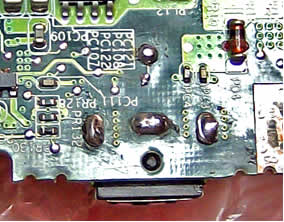
This is a view of the laptop power connector before the repair:
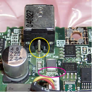
Inside the yellow circle is the main power connection from the connector to the board – note that you can see a dark circle completely around it, indicating that there is no solid metal connection.
Also note that it looks somewhat ‘burnt’ – this is indicative of sparking taking place. This connection carries 3 amps of current. The current then passes through the component labeled PF1 ( literally ‘Power Fuse 1’). It then is supposed to connect to this side of the part circled in red (‘PL1’) – but notice that flexing of the board as the connector was wiggled caused a crack you can see running horizontally under this end of this part.
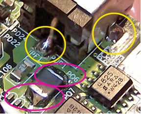
Same view, after the repair:

The green coating covering the metal leading up to the power connector was scraped off down to the bare copper of the board, in three places – the center pin, circled in yellow here, and the connector pins on both sides (see below). All were resoldered – on the top side of the board first, then touched up on the bottom (which is not where the primary electrical contact is made). The new broader, smoothly-tapered connection will be both physically stronger, and a better electrical connection.
Inside the red circle, you can see this was done for other part (PL1), as well.
Bottom view of connector, before the repair:
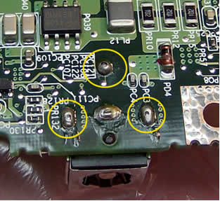
Again note that inside the circled areas, you can see dark circles where there should be solid metal, indicating that the original physical connection has been broken, and the parts are only transferring power due to the fact that they are touching . In fact, the only thing even holding the connector to the board is the connection in the bottom middle (between the two lower yellow circles) and it has a crack in it, as well.
Notice, also, the dried flux residue, indicating that this bottom-side soldering was done entirely, or touched up, by hand – and not cleaned afterwards.
The actual metal that conducts the power is actually of the top side of the board, where the connector is mounted, but the fact that the solder that flowed through mounting holes has cracked indicates is was not properly soldered in the first place.
As you can see in the two views below, all solder joints between the connector and the top side copper on the board now look much better. Increasing the size and coverage of the solder joints to the metal sides of the connector will make its mounting to the board physically much stronger as well, and better able to resist any side-to-side or up-and-down forces.
Inside the red circles, you can see that both sides of that part PL1 have been well resoldered.
This bottom view of the board after the repair shows good flow of solder through to the bottom side at the time the joints were resoldered.
No comments:
Post a Comment